Kirchoff's Current Law: The sum of currents entering a node equals zero. For an ideal JFET, no current flows between gate and source, or gate and drain. Thus, any current passing through passes between drain and source. Also question is, does current flow from source to drain?
4 Answers. Conventional current flows from Drain to Source in an N Channel MOSFET. The arrow shows body diode direction in a MOSFET with a parsitic diode between source and drain via the substrate. So diode has other polarity otherwise body diode would conduct whenever there was gate voltage.
One may also ask, how do you calculate drain current? To find out whether the MOSFET is biased in saturation, one first calculates the saturation voltage, VD,sat: The drain current is then obtained from: The transconductance equals: corresponding to a modified mobility mn* = 149 cm2/V-s.
Furthermore, what is drain current?
The drain current below threshold voltage is defined as the subthreshold current and varies exponentially with Vgs. The reciprocal of the slope of the log(Ids) vs. Vgs characteristic is defined as the subthreshold slope, S, and is one of the most critical performance metrics for MOSFETs in logic applications.
How increase drain current in Mosfet?
The MOS transistor is biased within the saturation region to establish the desired drain current which will define the transistors Q-point. As the instantaneous value of VGS increases, the bias point moves up the curve as shown allowing a larger drain current to flow as VDS decreases.
Related Question Answers
What is drain source and gate?
The very basics are that the gate, source and drain are terminals of a Field Effect Transistor(FET) , as opposed to the bipolar transistor where the equivalent terminals are the emitter, base and collector. The gate is the terminal that is used to control the flow of current through the FET. What is drain source voltage?
V(BR)DSS — Drain-source breakdown voltage V(BR)DSS (sometimes called BVDSS) is the drain-source voltage at which no more than the specified drain current will flow at the specified temperature and with zero gate-source voltage. Are source and drain interchangeable?
Short answer is YES. Source and Drain are interchangeable in schematic/layout. But once fabricated in silicon, they will be slightly different because of the doping process which is angular (not 90degrees) with respect to the silicon substrate, this makes the two terminals slightly different. What is drain and source?
Source and Drain are two Ohmic contacts through which a FET can interact with the outer world. Through source contact electrons can be supplied to the conducting channel of FET, where as through drain contact electrons can be collected from the conducting channel of the FET. Why is gate current zero in a Mosfet?
Gate current is Zero in MOS transistor always because gate terminal is isolated from substrate of mos transistor by an dielectric medium SiO2 . In simple words ,” MOSFET is formed by MOS CAPACITOR which is always in equilibrium under all condition . so no gate current can pass through it.” Can Mosfet conduct in both direction?
2 Answers. Yes it does conduct in either direction. Due to the body diode, most discrete MOSFETs cannot block in the reverse direction, but the channel will conduct in either direction when the gate is biased "on". If you want to conduct and block in both directions you need two MOSFETs in series. Does current flow through the gate of a Mosfet?
The gate of a MOSFET is composed of a silicon oxide layer. Since the gate is insulated from the source, an application of a DC voltage to the gate terminal does not theoretically cause a current to flow in the gate, except in transient periods during which the gate is charged and discharged. What is difference between enhancement mode and depletion mode?
Difference between enhancement and depletion type mosfet Depletion mode MOSFET is normally turned on at zero gate voltage. MOSFETs with enhancement modes are the common switching elements in most MOSs. These devices are deactivated at zero gate voltage and can be switched on by powering the gate. What is shorted gate drain current?
Shorted-gate drain current (IDSS) It is the drain current with source short-circuited to gate (i.e. VGS =0) and drain voltage (VDS) equal to pinch off voltage. It is sometimes called zero-bias current. The JFET circuit with VGS =0 i.e. source short circuited to gate and is normally called shorted-gate condition. What is Drain saturation current?
A depletion layer located at the drain end of the gate accommodates the additional drain-to-source voltage. This behavior is referred to as drain current saturation. Drain current saturation therefore occurs when the drain-to-source voltage equals the gate-to-source voltage minus the threshold voltage. What is drain current JFET?
Electric current from source to drain in a p-channel JFET is restricted when a voltage is applied to the gate. Unlike bipolar transistors, JFETs are exclusively voltage-controlled in that they do not need a biasing current. Electric charge flows through a semiconducting channel between source and drain terminals. Why drain current is constant in saturation region?
The reason why it saturates is that there will be a region of higher resistance of size proportional to the Drain-Source voltage, and therefore the resistance of this region will be proportional to the same voltage. But as current is voltage/resistance, the dependence will cancel out and you'll get "constant" current. What is GM in Mosfet?
Transconductance is the property of certain electronic components. Conductance is the reciprocal of resistance; transconductance is the ratio of. the current change at the output port to the voltage change at the input port. It. is written as gm. Do MOSFETs have a voltage drop?
MOSFET: When the gate voltage is large with respect the the threshold voltage Vth, the voltage drop from drain to source is linearly dependent on current (for small voltages << Vth of the MOSFET), so it behaves like a resistor. BJT: Voltage drop from collector to emitter is dependent on current but not linearly. What is K in Mosfet?
= The Process Transconductance Parameter k′ is a constant. that depends on the process technology used to fabricate an integrated circuit. Therefore, all the transistors on a given substrate will typically have the same value of this parameter. The Channel Aspect RatioW L is simply the ratio of channel. What is the symbol of Mosfet?
The line in the MOSFET symbol between the drain (D) and source (S) connections represents the transistors semiconductive channel. If this channel line is a solid unbroken line then it represents a “Depletion” (normally-ON) type MOSFET as drain current can flow with zero gate biasing potential. What is pinch off voltage?
Pinch off voltage: Pinch off voltage is the drain to source voltage after which the drain to source current becomes almost constant and JFET enters into saturation region and is defined only when gate to source voltage is zero. What is on current in Mosfet?
@Sanjib: Gate current is not a leakage current in a MOSFET. In the on-state, the current flowing between the source and drain is the on-current. Gate current occurs due to the discharge of the capacitor during the transient condition. What is an NMOS transistor?
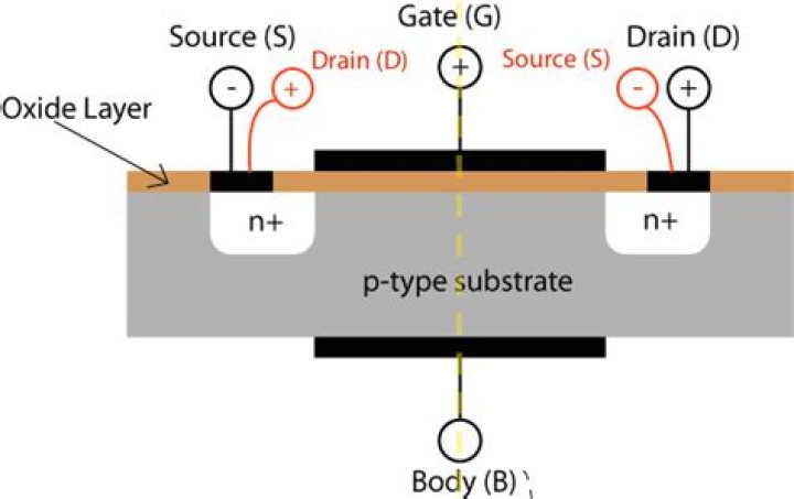
NMOS Transistor. A Metal-Oxide-Semiconductor Field-Effect Transistor(MOSFET) is a four terminal device whose terminals are named as Gate(G), Drain(D), Source(S) and Bulk(B). The positive voltage attracts free-floating electrons within the body towards the gate, forming a conductive channel. When VGS reaches to threshold voltage drain current is?
First, the threshold voltage VGS(th) is not intended for system designers. It is the gate voltage at which the drain current crosses the threshold of 250 μA. It is also measured under conditions that do not occur in real-world applications. How is GM calculated in Mosfet?
For vacuum tubes, transconductance is defined as the change in the plate(anode) current divided by the corresponding change in the grid/cathode voltage, with a constant plate(anode) to cathode voltage. Typical values of gm for a small-signal vacuum tube are 1 to 10 millisiemens. What is linear region in Mosfet?
Linear mode operation refers to the current saturation region in the output characteristics. The drain current (IDS) is nearly independent of the drain to source voltage (VDS) for a given gate to source (VGS) voltage. It depends then directly on the VGS- voltage of the MOSFET. Here, the MOSFET operates in linear mode. What is drain current in Mosfet?
The drain current below threshold voltage is defined as the subthreshold current and varies exponentially with Vgs. The reciprocal of the slope of the log(Ids) vs. Vgs characteristic is defined as the subthreshold slope, S, and is one of the most critical performance metrics for MOSFETs in logic applications. How do MOSFETs amplify current?
MOSFETs are controlled by voltage, so NO, not on their own. It is possible to amplify current using a MOSFET - pass the input current through a resistor, so convering the current signal to a voltage. Then use that signal voltage to control the MOSFET, which will give an output signal current. How Mosfet works as an amplifier?
The advantage of the voltage divider biasing network is that the MOSFET, or indeed a bipolar transistor, can be biased from a single DC supply. Therefore if we apply a small AC signal which is superimposed on to this DC bias at the gate input, then the MOSFET will act as a linear amplifier as shown. What is a gate voltage?
The gate-source voltage, VGS, of a FET transistor is the voltage that falls across the gate-source terminal of the transistor, as shown above. The gate-source voltage, VGS, is a very important voltage because it is the voltage which is responsible for turning off a JFET or a depletion MOSFET transistor. What is the working of Mosfet?
Working Principle of MOSFET It works by altering the width of the channel through which the movement of charge carriers (electrons for N-channel and holes for P-channel) occurs from source to drain. The gate terminal is insulated whose voltage regulates the conductivity of the device. What is CMOS logic?
CMOS. Stands for "Complementary Metal Oxide Semiconductor." It is a technology used to produce integrated circuits. These two semiconductors work together and may form logic gates based on how the circuit is designed. What is the symbol of FET?
Junction FETs or JFETs were the first type of FET and these have a distinctive symbol showing the diode junction. Insulated gate FETs, including MOSFETs have circuit symbols that indicate the insulation on the gate.